
Services typically provided within a project

First of all, the requirements are captured, as they define the actions needed to accomplish the project, whether the project is small or large. The set of requirements gives an idea of the scope of work and guidelines for planning.

The analysis of requirements is done to ensure all aspects of design are covered and enable to create a product with features traceable to requirements.

Once the set requirements is approved, the concept ideas are proposed allowing to choose the best way of building a product.

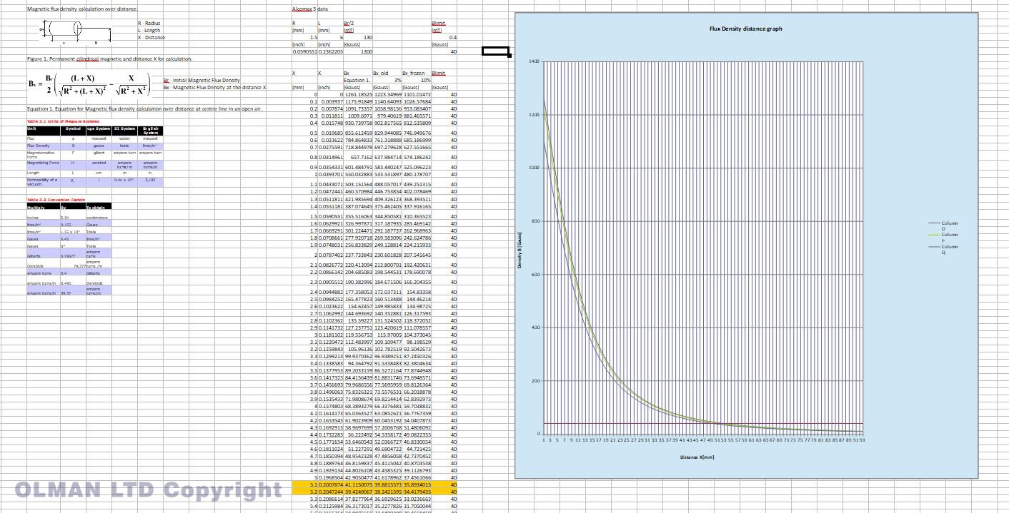
The critical calculations are made upon conceptual chose, which allows to see the off the shelf parts suitable for design and limitations.
All previous steps allow to perform a feasibility study answering whether the chosen concept is possible to build in real world.

Planning is done to get an idea about resources, funds and time needed for bringing the idea to real life.

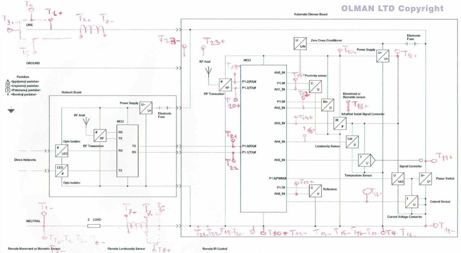
The design architecture is produced revealing the interlinked components of entire design.

The algorithms add an intelligence and create IP of the product.

Components are selected for the design utilizing de-rating criteria, which allows robust design operation under specified electrical and environmental conditions.
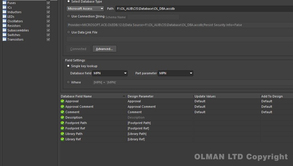
New component libraries are created filling in required parameters in a database library, allowing further stress analyses for safety critical operation.
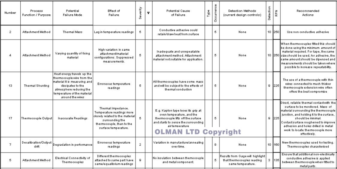
In case there is some uncertainty in a complex system, then Failure Mode & Effect Analysis is done to investigate possible failure modes and their remediation.

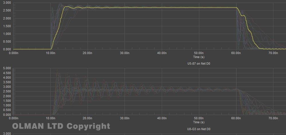
Simulation models are created and simulation is done for critical circuits.

Mechanical aspects of design and components are considered and collision verification is done.

The schematic is captured following logical hierarchy of a concept's architecture.

The firmware is configured, verified and programmed on PSoC and FPGA devices allowing most effective use of resources.

A PCB artwork is done upon successful schematic review.
Signal integrity analysis performed for the high speed and EMC sensitive PCB designs.
After PCB approval, the fabrication files are generated allowing PCB fabrication.

The PCB assembly files are generated allowing PCB population.

A commissioning of assembled PCBs is done and Printed Board Assembly performance is brought to specified level.

Embedded coding is done on commissioned PBA adding intelligence and intellectual property.

The tests are done through out the circuits gathering the required data and validating the design.

The design functions are debugged, bringing it up to specification, if necessary.
The design features, circuits and modules are verified against the requirements assuring confidence of product's performance.

Finally, the product pre-certified by performing EMC, EMI and safety tests increasing confidence for further certification.